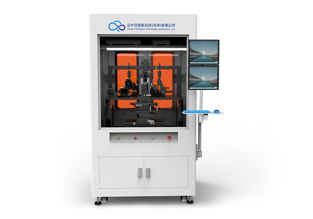

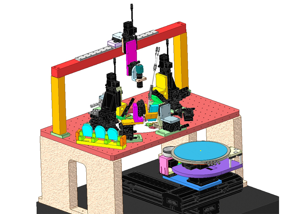
Semi automatic/fully automatic high-precision probe station
Piezoelectric motion system
Hexapod Movement System
Probe card device
Instrument control cabinet
Camera positioning system
laser range finder
IPC
Control and testing software
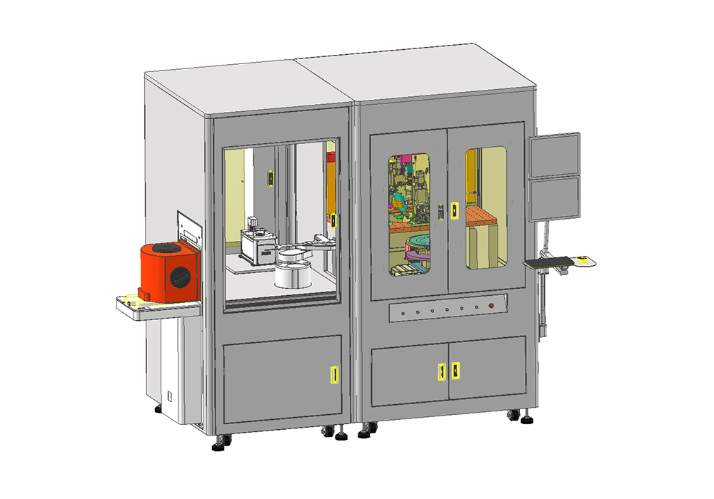
Provide semi-automatic and fully automatic loading and unloading solutions for silicon wafer testing platforms.
Main configuration:
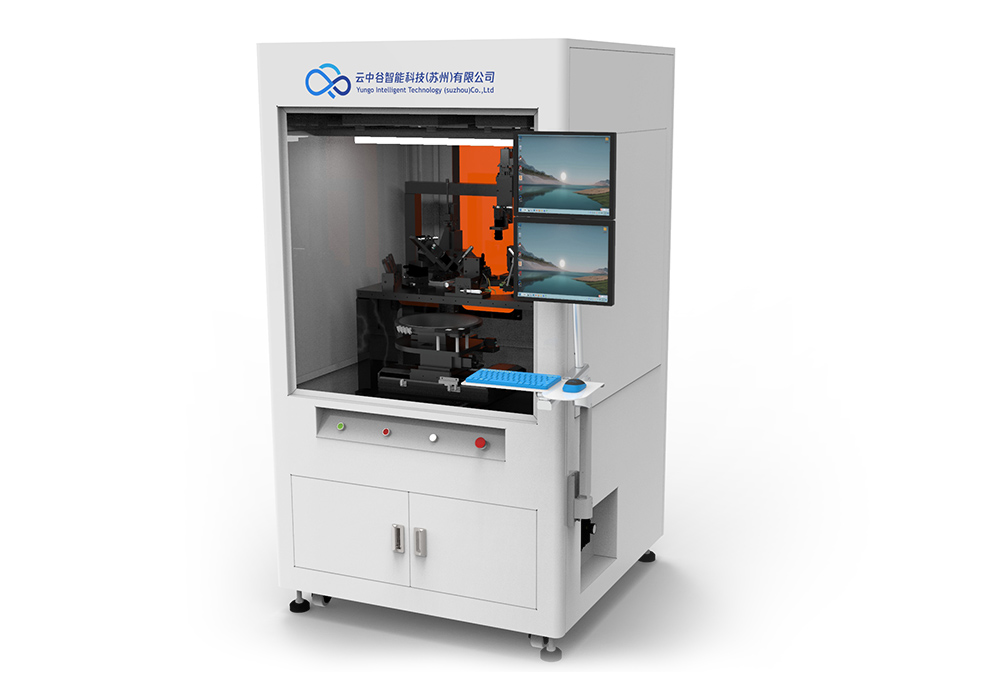
Semi automatic/fully automatic high-precision probe station
Piezoelectric motion system
Hexapod Movement System
Probe card device
Instrument control cabinet
Camera positioning system
laser range finder
IPC
Control and testing software
Parameters:
1. Suitable for 8-inch wafers, compatible with 6-inch wafers, other sizes require additional customization;
2. Test content: optical and electrical measurements of coupling efficiency, insertion transmission loss, polarization loss, wavelength, 3dB bandwidth, PD performance, etc;
3. Use high-resolution cameras to achieve Die positioning and FA positioning
4. MAP maps and files can be generated according to customer requirements; Multi Bin classification display Mapping function;
5.RT~+ 200℃ ;
6. The coupling repetition accuracy is less than 0.2dB; the coupling time per die is less than 2.5S (search distance is less than 400 microns);
7. Air floating vibration isolation platform (configured with shock absorption scheme according to customer needs);


No. 1798, Zhonghua Yuan West Road, Yushan Town, Kunshan City, Suzhou City
Copyright © 2025 Cloud Valley Intelligent Technology (Suzhou) Co., Ltd All Right Reserved